
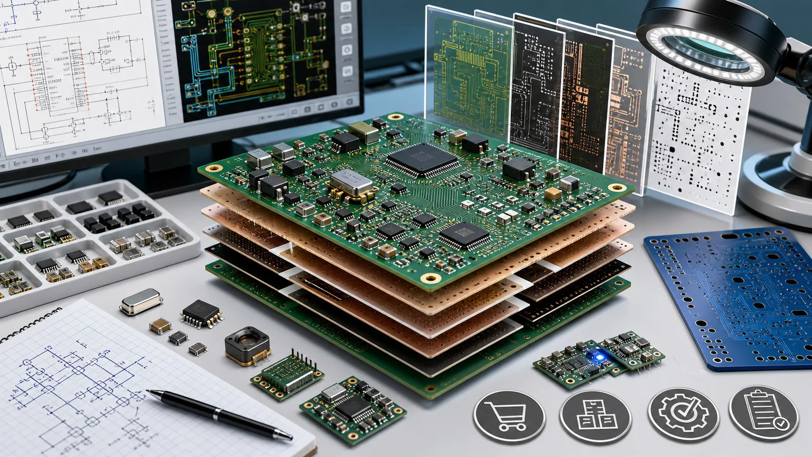
BoostCore-Module
BoostCore-Module is a compact adjustable DC-DC step-up boost converter module built around the MT3608 regulator.
It supports USB-C 5V input, an optional external VIN input, Schottky OR-ing input selection, resettable fuse protection, TVS protection on USB VBUS, and a trimpot-adjustable output feedback network.
PCB manufacturing sponsor: This project is sponsored by PCBWay.
PCBWay support is mentioned in the documentation because the PCB is intended to be published as an open hardware project and manufactured as a compact prototype board.
Project Highlights
- MT3608 based boost converter
- USB-C power-only input
- External VIN input
- Input OR-ing with SS36 Schottky diodes
- USB-C VBUS protection with 5V TVS diode
- USB-C PTC fuse protection
- Optional VIN_EXT PTC fuse protection
- Adjustable output voltage using trimpot
- 0805 resistor/LED-friendly design choices
- Test points for VIN, VOUT, FB, EN and GND
- KiCad-ready hardware folder structure
- GitHub documentation package with BOM, assembly, layout and testing guides
Sponsorship
This project is sponsored by PCBWay.
PCBWay is mentioned here as the PCB manufacturing sponsor for the open hardware release of BoostCore-Module. The board was designed with prototype manufacturing in mind, including compact routing, silkscreen labels, test points, and an export-ready project structure.
Electrical Overview
| Parameter | Value |
|---|---|
| Controller IC | MT3608 |
| Topology | Boost / step-up |
| USB-C input | 5V only |
| External VIN input | 2V-24V target range |
| Output voltage | Adjustable by RV1 trimpot |
| Switching frequency | MT3608 typical 1.2MHz |
| Inductor | 4.7uH recommended |
| Main boost diode | SS36, 3A, 60V |
| Output adjustment | R1 + R2 + RV1 feedback network |
| Output capacitor caution | Use 50V capacitors for high output voltage |
Current Feedback Network
The adjustable output stage is:
VOUT -> R2 10k -> RV1 100k trimpot -> FB -> R1 2.2k -> GND
Recommended trimpot wiring:
RV1 pin 3 -> R2 side
RV1 pin 1 + pin 2 -> FB node
Formula:
VOUT = 0.6 x (1 + R_UPPER / R1)
Where:
R_UPPER = R2 + active RV1 resistance
R1 = 2.2k
Important:
- Start with the trimpot at the lowest output setting.
- Always adjust output using a multimeter.
- Do not connect a sensitive load before confirming VOUT.
- High output voltages require output capacitors rated above the selected voltage.
Images
Layout preview
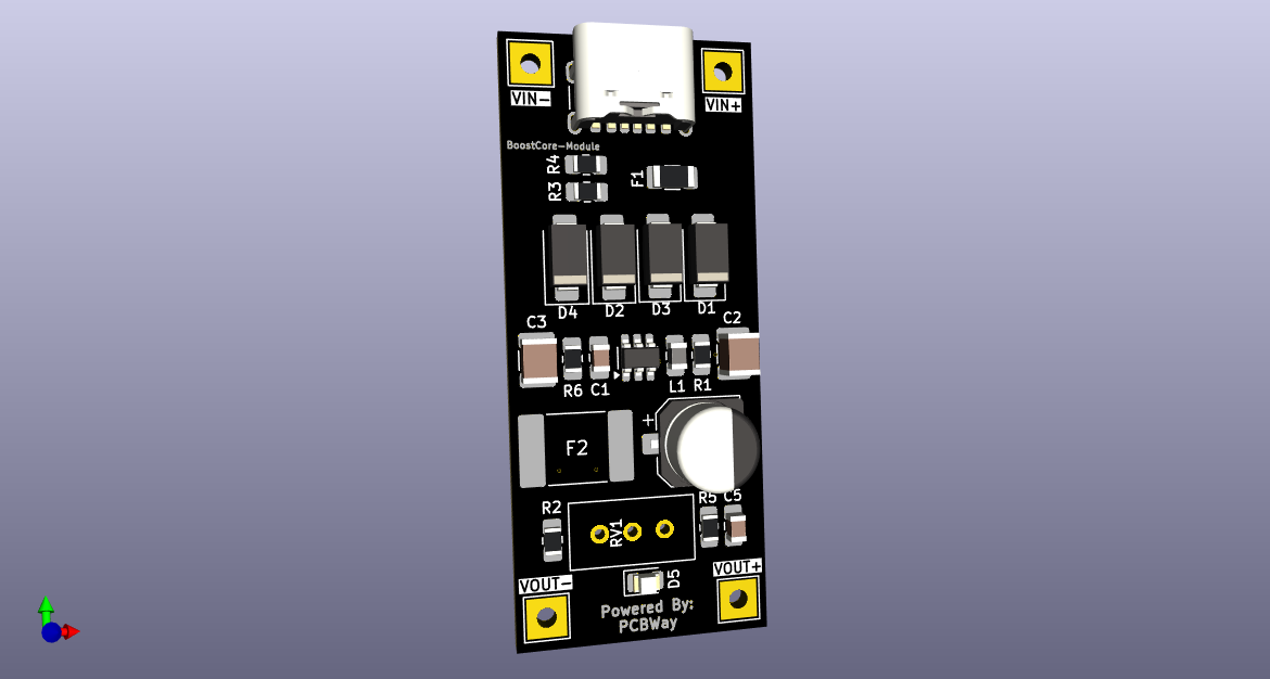
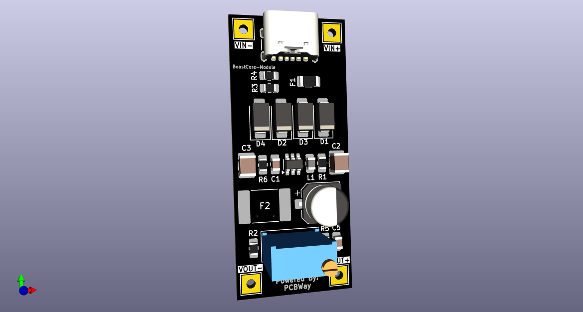
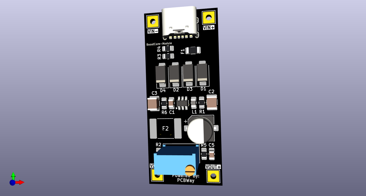
Important Hardware Notes
USB-C input
The USB-C connector is used as a 5V power-only input.
Required CC resistors:
CC1 -> 5.1k -> GND
CC2 -> 5.1k -> GND
USB-PD negotiation is not implemented. The USB-C input is therefore 5V only.
F1 USB fuse
Current selected part:
F1 = KLM3S300RY
PTC resettable fuse
1206 / 3A / 6V
USB-C 5V input only
Do not use this part on the 24V external input path.
F2 external VIN fuse
Compact option:
F2 = MF-MSMF110/24X-2
1812 / 1.1A / 24V
Higher-current but larger option:
F2_ALT = FSMD185-2920-R
2920 / 1.85A / 33V
D2 USB TVS
D2 must be a 5V TVS diode, not a Schottky diode.
Recommended:
D2 = P4SMAJ5.0_R1_00001
D1 / D3 / D4
The board uses SS36 diodes:
D1 = SS36
D3 = SS36
D4 = SS36
D3 and D4 are used for input OR-ing.
C4 polarity
If using the compact electrolytic output capacitor:
C4 (+) -> VOUT
C4 (-) -> GND
Mark polarity clearly on silkscreen.
PCB Layout Rules
Boost converters are layout-sensitive. Follow these rules:
- Keep the SW node as short and small as possible.
- The SW node is:
U1 pin 1 SW + L1 right side + D1 anode - Do not place copper pour under the SW node area.
- Keep FB trace away from SW node, diode switching node and inductor.
- Place C1 close to U1 IN and GND.
- Place output capacitors close to D1 cathode and GND.
- Use a solid GND plane on the bottom layer.
- Add via stitching near high-current GND return paths.
- Do not route feedback under the inductor.
- Make VIN_SYS and VOUT traces wide.
Assembly Order
Recommended assembly sequence:
- Inspect PCB visually.
- Solder USB-C connector.
- Solder protection parts: F1, D2, D3, D4.
- Solder MT3608.
- Solder inductor L1 and diode D1.
- Solder resistors and small capacitors.
- Solder RV1 trimpot.
- Solder output capacitors.
- Solder connectors.
- Inspect polarity of C4.
- Check shorts between VIN, VOUT and GND.
- Power on without load.
- Adjust output voltage with a multimeter.
- Test with a dummy load.
First Power-Up Checklist
Before applying power:
- Check USB-C VBUS is not shorted to GND.
- Check VIN_SYS is not shorted to GND.
- Check VOUT is not shorted to GND.
- Confirm D1 cathode points to VOUT.
- Confirm C4 polarity.
- Confirm RV1 pin 1+2 go to FB.
- Confirm RV1 pin 3 goes to R2.
- Confirm EN is pulled to VIN_SYS through R6.
Initial test:
1. Apply input power.
2. Measure VIN_SYS.
3. Measure VOUT.
4. Adjust RV1 slowly.
5. Verify output under light load.
6. Check temperature of MT3608, L1 and D1.
License
Released as open hardware documentation. See LICENSE.
Disclaimer
This is an open hardware project. Use at your own risk. Verify all footprints, ratings, clearances, capacitor voltage ratings and component stock before fabrication or ordering.